This article briefly examines the basic features of input-output blocks inside the field-programmable gate array devices and how these features potentially may limit the number of external components in the PCB design. The article is directed to readers acquainted with general purpose processors and microcontrollers and willing to compare the PCB design effort with the FPGA. Since FPGA architecture differs from vendor to vendor, Spartan 6 family from Xilinx has been chosen as an off-the-shelf product example.
About the FPGA
FPGA has over 30 years’ history and has proven to be a powerful technology with a wide range of applications. FPGA devices evolved from the old programmable logic arrays and now they fill the gap between general purpose processors and ASICs. General purpose processors have a fixed nature (a limited number of registers and a fixed instruction set) whilst ASICs have issues which make the design time-consuming, high-risk and thus very expensive.
The internal structure of FPGA may be very complex and its building blocks can vary from family to family. However, typically, it consists of many configurable logic blocks, each containing a collection of ‘flip-flops’, look-up tables and carry logic.
As well as these logic blocks, ready-to-use blocks are provided within the chips – especially RAM memory blocks, DSP blocks, clock generation units and even more complicated gear such as DRAM memory controllers. In fact perhaps the most substantial part of the FPGA is a set of configurable input-output blocks because, all in all as any device in the system, the FPGA can be treated as a black-box with some inputs and some outputs.
I/O flexibility of the FPGA
The FPGA is highly customisable and this is its greatest asset. Any behaviour can be defined – typically, in hardware description language such as Verilog and VHDL – synthesised and run, provided some spatial (for example, maximum number of logic cells utilised) and timing (signal propagation time limits) constraints are met.
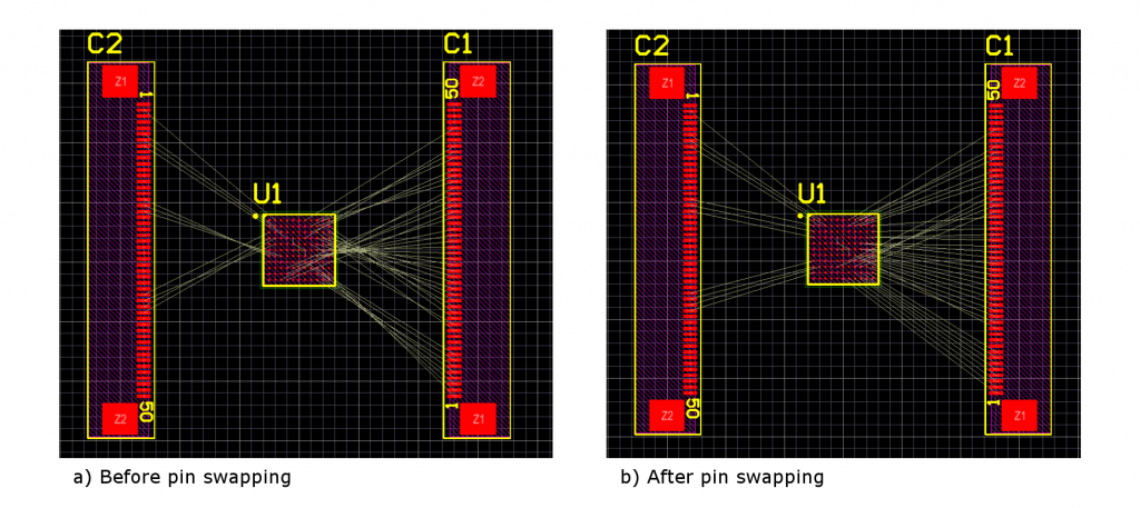
The FPGA flexibility does not omit the pin assignment; this is very useful for the PCB engineer, especially when the EDA tool supports an automatic or semi-automatic pin reassignment. The state-of-the-art EDA software is able to synchronize HDL-based design, schematics and PCB layout and be aware of hardware constraints of the particular FPGA device. For example the software can not break differential pairs, power supply domains or constraints related to special function of the pin like global clock input. From the example in the picture below (a), one can see an hypothetical situation where signals were assigned in a non-optimal way. This may lead to the:
- unnecessary hindering of the PCB routing process (which affects costs).
- increase in the number of copper layers (which affects the costs).
- degradation of electrical properties of the signal traces, especially in high-speed interfaces (which also affects the costs, most notably when we run into trouble with EMI).
The picture (b) shows the result of signal unravelling which, effectively, decreased number of intersections in so called ratsnest.
IOB features
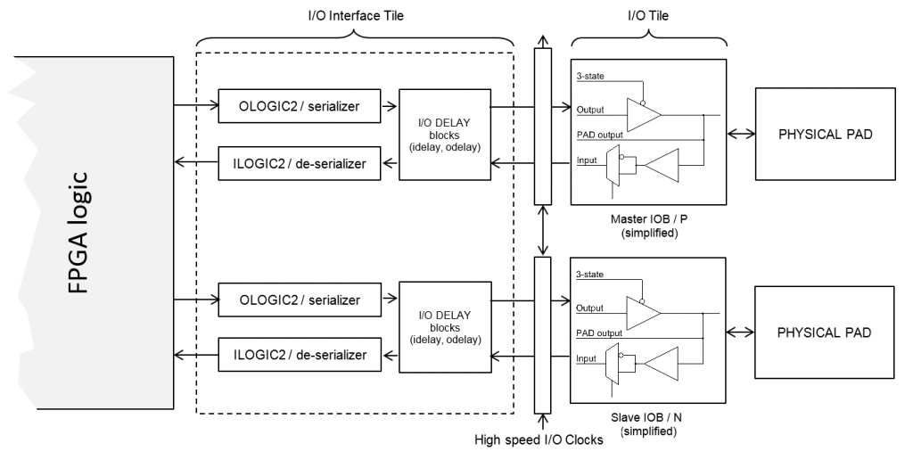
As it was mentioned FPGA internals differ from vendor to vendor. As en example, let’s look at the popular Spartan-6 family. A very detailed description of the input-output capabilities can be found in Spartan-6 FPGA Select IO Resources (UG381) user guide. Most important building-blocks of the I/O logic has been depicted below.
The I/O interface tile contains advanced blocks for signal phase shaping (needed by DRAM interfaces), delaying and both serial-to-parallel and parallel-to-serial bit stream conversion. Each of these blocks could be a topic for another article and will not be described further. Actually the electrical behaviour of FPGA pad is defined by IOB configuration. The reason why IOB appear in pairs is that they may work in master-slave configuration, i.e. when differential signal has been configured.
Typically, the function of the I/O block is defined in a special constraint file when using HDL synthesis tool. The basic usage of the input-output block is very similar to what can be achieved in the world of microcontrollers. This usage has been summarised in the table below:
| FPGA I/O function | Microcontroller’s equivalent |
|---|---|
| input buffer | general purpose input |
| output buffer | general purpose output |
| bidirectional mode | switching GPIO mode (needs a little help of software) |
| 3-state output buffer | switching GPIO direction (needs a little help of software) |
| differential input/output/bidirectional/3-state buffer | rarely found as GPIO, if at all |
Apart from this fundamental configuration there is a lot of additional constraints that allow to ‘shape’ the electrical characteristics of the signal interface.
I/O standard for instance defines the signalling standard and voltage levels. In spite of huge amount of supported I/O standards it is quite obvious that their usage is limited to the voltage used to supply the I/O cell. One needs to mention here the I/O tile arrangement. They are organized into banks, each of them having separate power supply, thus supporting different sets of I/O standards. Popular standards are listed in the table below (this is not a complete list):
| I/O standard family examples | Typical usage |
|---|---|
| TTL / CMOS | general purpose |
| SSTL/HSTL (different classes) | SRAM / SDRAM / DDR interfaces |
| LVDS | high speed differential communication |
| TMDS | DVI/HDMI |
| Dedicated usage standards | PCI, I2C, SDIO |
Please note that it is uncommon for microcontrollers to allow mapping from specialised peripherals such as SDRAM controller, LCD, SPI, etc to any available pin resource. Excluding the cases of quite high freedom in peripheral multiplexing (a good example may be PIC24FJ256DA210 from Microchip), the usual way is to provide inputs and outputs to a very limited number of pins (see alternative function of GPIO in any STM32 microcontroller).
Another constraint allows to declare the weak pull-up and pull-down resistor or the less popular bus keeper. For signal integrity purposes, drive strength and slew rate control is available. Although, these features can easily be found in STM32 microcontrollers, the FPGA usually has more degrees of freedom (meaning finer drive strength customisation).
The most interesting feature improving PCB complexity is the on-chip termination. This is very crucial in high speed interfaces. Although some of the interfaces mentioned in the user guide require external termination, a lot can be done inside the chip:
- the output buffer impedance can be programmed to match the transmission line impedance (25, 50, 75 Ohm).
- input split termination can be enabled with above values.
- differential termination with fixed value 100 Ohms (for interfaces like LVDS).
FPGA devices are highly customisable in terms of I/O assignment and thus able to simplify the components placement process in the PCB design. In many cases the input-output blocks inside the FPGA let the PCB engineers limit unnecessary components like weak pull resistors or external termination. The IOB can easily perform task of GPIO with some additional features like finer slew rate and drive strength customisation, optional termination, differential signaling and different voltage levels support.


